
information centre / Industry Information / High-precision ceramic mirror substrates – the industrial choice for precision and quality.
High-precision ceramic mirror substrates – the industrial choice for precision and quality.
Introduction
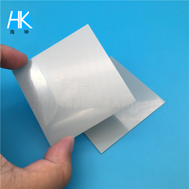
In high-end fields such as semiconductor manufacturing, optical components, new energy electronics, and precision medical equipment, surface flatness and mirror finish directly determine product performance and yield. Traditional materials struggle to balance high flatness, low roughness, and long-term stability, making high-precision ceramic mirror substrates the industry’s preferred choice. We offer alumina ceramic, silicon nitride ceramic, and aluminum nitride ceramic substrates, employing precision grinding and mirror polishing processes to achieve high-performance, high-stability mirror substrate solutions.
Quick Links
Contact Us
Live
E-mail:sales01@hkceramic.com
Why choose precision ceramic mirror substrates?
1. Extremely low surface roughness
Achieving a Ra of 0.02μm for a super-mirror finish
Ensuring the processing quality of semiconductors, optical components, and precision electronic devices
Reducing the risks of subsequent processing and assembly
2. Ultra-high flatness
Maximum flatness up to 0.001mm
Accuracy is dimension-dependent and can be customized to customer requirements.
Ensuring high consistency between wafers, optical substrates, and electronic components.
3. Stable physical properties
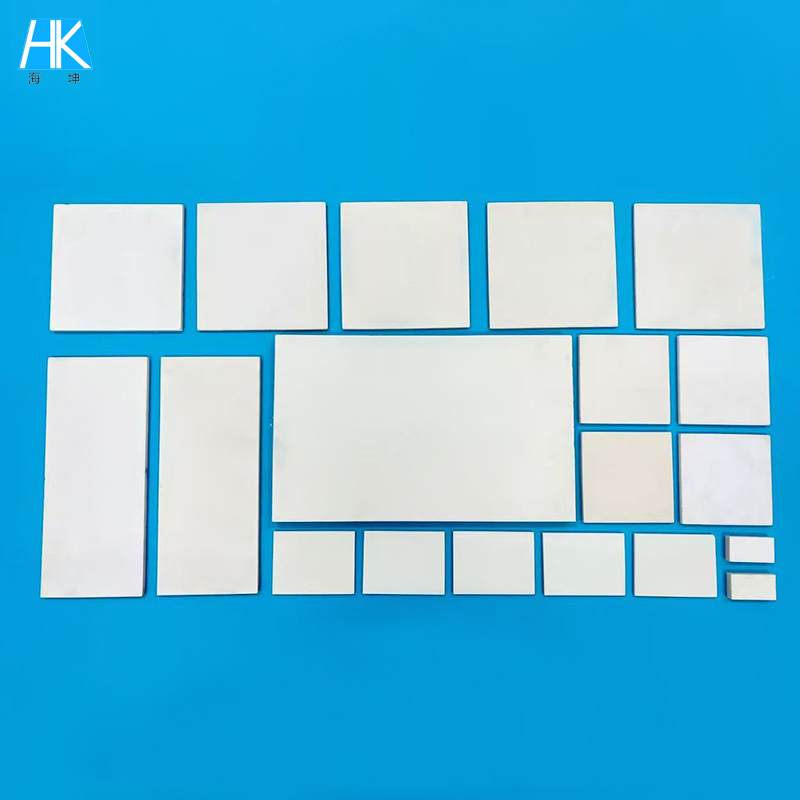
Alumina ceramics: high cost-performance ratio, wear-resistant and corrosion-resistant, suitable for a variety of industrial applications.
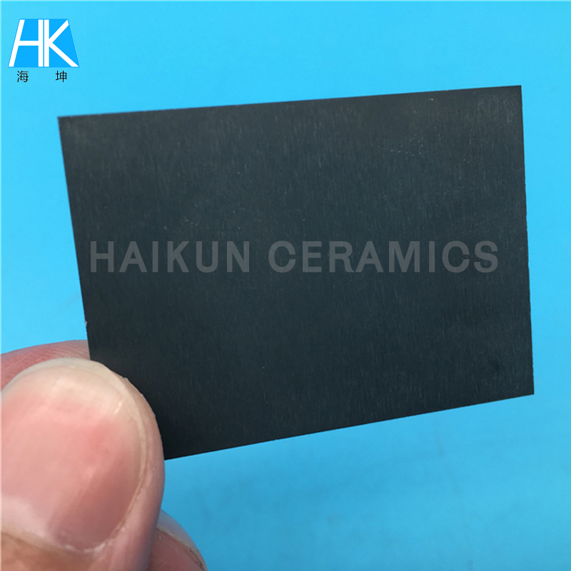
Silicon nitride ceramics: high thermal stability, high strength, and high toughness, suitable for high-load processing.
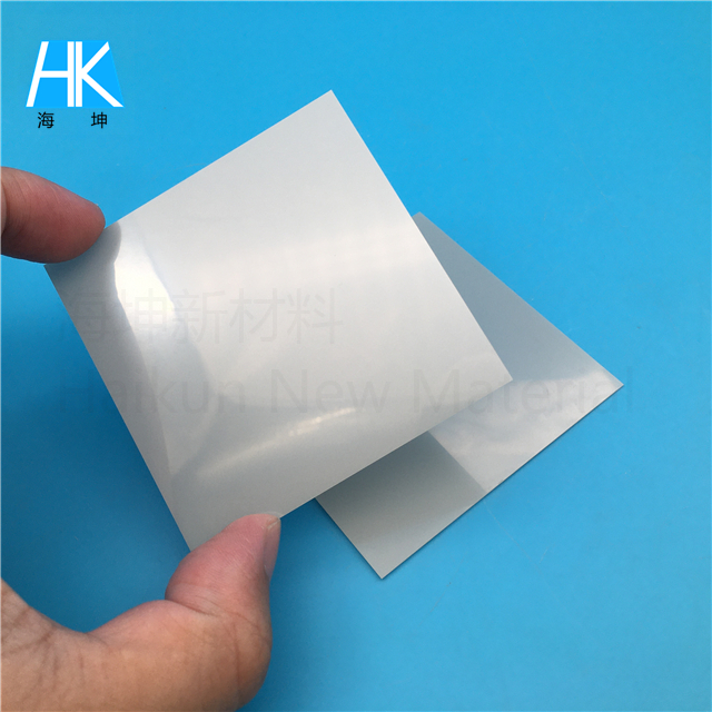
Aluminum nitride ceramics: high thermal conductivity and excellent insulation, suitable for the electronics and semiconductor industries.
4. High-precision machining capabilities
Custom sizes and thicknesses supported
Integrated precision grinding and mirror polishing
Strict tolerance control to meet micron-level application requirements
Application areas
High-precision ceramic mirror substrates are widely used in:
Semiconductor wafer carriers and precision supports
Optical glass, sapphire, and lens substrates
Precision electronic devices and sensors
High-end medical device components
Laser and optoelectronic equipment
New energy electronics industry
Advantages of precision machining
| characteristic | Process capabilities | Customer Value |
|---|---|---|
| Mirror surface (highest) | Ra0.02μm | Improve optical/electronic processing performance |
| Flatness (highest) | 0.001mm | Ensure high consistency and precision assembly |
| Material diversity | Al₂O₃, Si₃N₄, AlN, etc. | To meet different thermal, mechanical, and thermal conductivity requirements |
| Custom sizes | Multiple thicknesses available | Custom production is available based on drawings. |
| stability | High temperature/high load/long-term use | Extend substrate lifespan |
⚠Note: Precision is related to structure and size, and can be customized according to customer drawings and technical requirements.
Why are Hyde's ceramic mirror substrates trustworthy?
Over 20 years of experience in precision ceramic machining
Advanced grinding and mirror polishing processes
Strict dimensional and tolerance management
Small batch prototyping and mass production available
OEM/ODM customization supported
Whether in the semiconductor, optics, electronics, or medical industries, our ceramic mirror substrates can meet the stringent requirements of high precision, high flatness, and high stability.
Contact Us
If you are looking for high-precision ceramic mirror substrates, please contact us and submit your drawings or specifications. We will provide:
Customized material solutions
Precision machining technology evaluation
Sample production and mass production services
Providing reliable, high-quality core material support for your high-end manufacturing projects.
Relevant information