information centre / Industry Information / What are the common sizes for ceramic substrates? How should they be selected for different applications?
What are the common sizes for ceramic substrates? How should they be selected for different applications?
Introduction
In the fields of electronic packaging, power modules, LED lighting, and semiconductor equipment, ceramic substrates are widely used in various high-reliability electronic devices due to their excellent thermal conductivity, insulation properties, and high-temperature stability. However, during actual procurement or design, many engineers encounter a question: What are the common sizes of ceramic substrates? Are there standard specifications? In fact, ceramic substrates have both common sizes and can be customized according to application requirements. Below, we will provide a detailed introduction from three aspects: commonly used industry specifications, the size range of different materials, and customization capabilities.
Quick Links
Contact Us
Live
E-mail:sales01@hkceramic.com
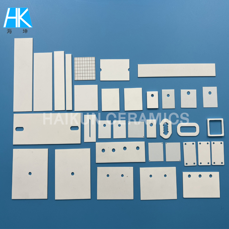
1. Common standard dimensions of ceramic substrates
In the electronics industry, many ceramic substrates use relatively standardized dimensions for ease of fabrication and circuit design. Common dimensions include:
| Common sizes (mm) | Application areas |
|---|---|
| 10 × 10 | Microelectronic devices, small modules |
| 20 × 20 | Sensors, circuit modules |
| 30 × 30 | LED substrates, small power devices |
| 50 × 50 | Power electronics, power modules |
| 100 × 100 | Power modules, IGBT packages |
| 114 × 114 | Semiconductor equipment, power devices |
| 120 × 120 | High-power heat dissipation module |
These dimensions are very common in the LED packaging, power module, and power electronics industries.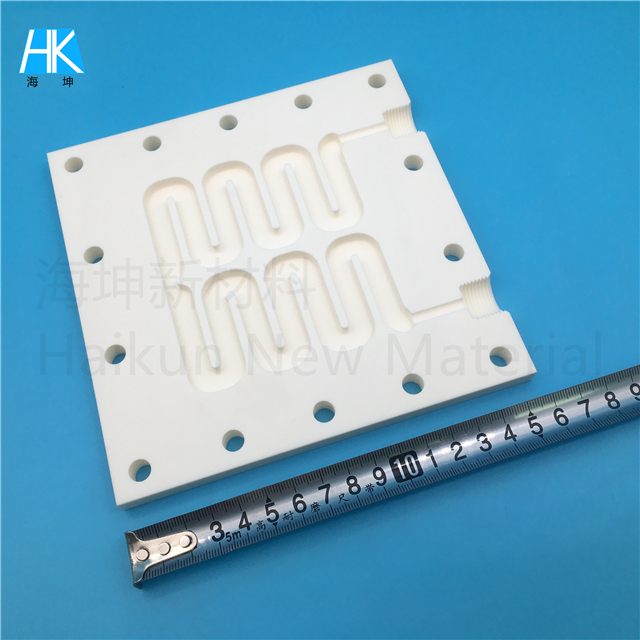
2. Common thickness range of ceramic substrates
Besides length and width, thickness is also an important parameter for ceramic substrates. Different thicknesses directly affect strength, heat dissipation capacity, and processing costs.
Common thicknesses include:
| thickness | Typical applications |
|---|---|
| 0.25 mm | microelectronic circuits |
| 0.38 mm | Small power modules |
| 0.5 mm | LED heat dissipation substrate |
| 0.63 mm | Power Electronics |
| 1.0 mm | High-strength structural substrate |
| 1.5 mm | High power module |
In practical applications, 0.38mm, 0.5mm, and 0.63mm are the most common thickness specifications.
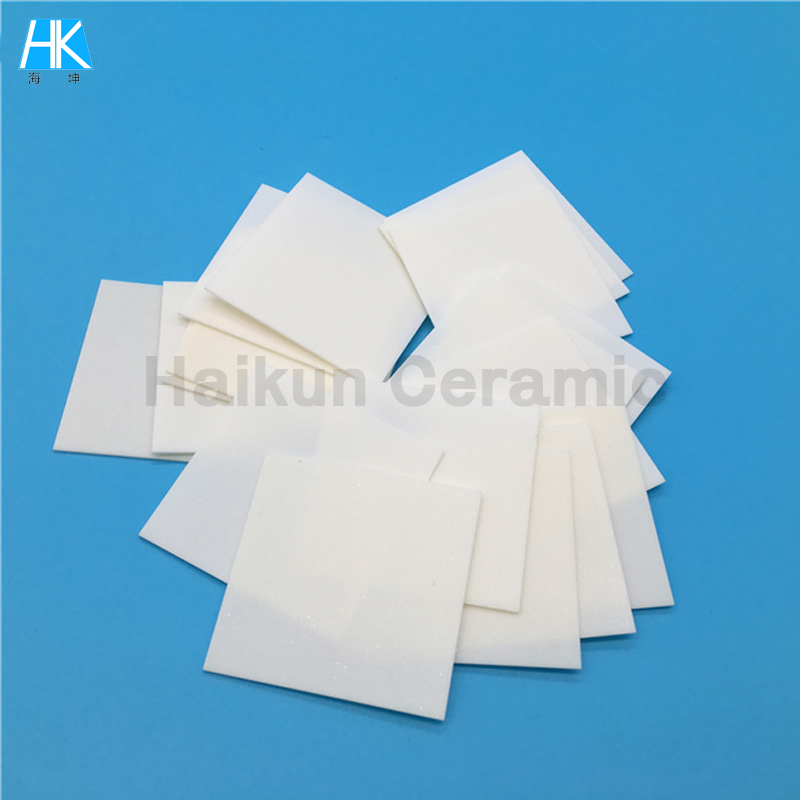
3. Size differences of ceramic substrates made of different materials
Different ceramic materials also vary in their dimensional capabilities.
1. Alumina ceramic substrate (Al₂O₃)
The most common electronic ceramic substrate material.
Features:
Low cost
Mature processing technology
Wide size range
Common size range: 10 mm ~ 200 mm
Common thickness: 0.25 mm ~ 3 mm
2. Aluminum nitride ceramic substrate (AlN)
Aluminum nitride has extremely high thermal conductivity, so it is widely used in power electronics and semiconductor heat dissipation.
Common size range:
20 mm ~ 150 mm
Common thicknesses:
0.3 mm ~ 2 mm
 3. Silicon nitride ceramic substrate (Si₃N₄)
Silicon nitride ceramic substrates have higher strength and better thermal shock resistance.
Common sizes: 30 mm ~ 120 mm
Common thickness: 0.32 mm ~ 1 mm
4. Why do ceramic substrates need to be customized in size?
While some common specifications exist, most ceramic substrates still require custom fabrication in practical industrial applications. The main reasons include:
Different circuit layouts
Different power module structures
Heat dissipation design requirements
Package size limitations
Therefore, ceramic substrates typically support:
Laser cutting
Precision grinding
Hole drilling
Special shape machining
Modern ceramic processing technology can achieve the following:
Dimensional tolerance ±0.02 mm
Micro-hole machining (0.1 mm or even smaller)
Complex irregular structures
4. What needs to be considered when selecting the size of the ceramic substrate?
When designing and sourcing ceramic substrates, it is recommended to focus on the following factors:
1. Power Density
The higher the power, the larger the heat dissipation area, and the larger the substrate size is usually required.
2. Circuit Layout
The complexity of the circuit layout will affect the design of the substrate size.
3. Heat dissipation requirements
The choice of material (alumina or aluminum nitride) also affects the dimensions.
4. Mechanical Strength
The greater the thickness, the higher the bending strength, but the cost will also increase.
5. Summary: Ceramic substrate dimensions are available in both standard and custom sizes.
In general, the common size range for ceramic substrates is as follows:
10 mm – 150 mm (general electronic applications)
Thickness 0.25 mm – 1.5 mm (most common)
As electronic devices develop towards higher power and higher density, the design of ceramic substrates is becoming increasingly customized to meet specific needs.
Therefore, when selecting a ceramic substrate, the most important thing is to design it reasonably according to the specific application scenario, rather than simply applying a fixed size.
Relevant information