Products / Alumina ceramics / Custom Laser Cut Alumina Ceramic Substrates Manufacturer
ProductMaterial properties
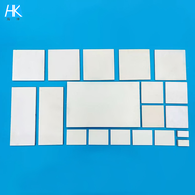
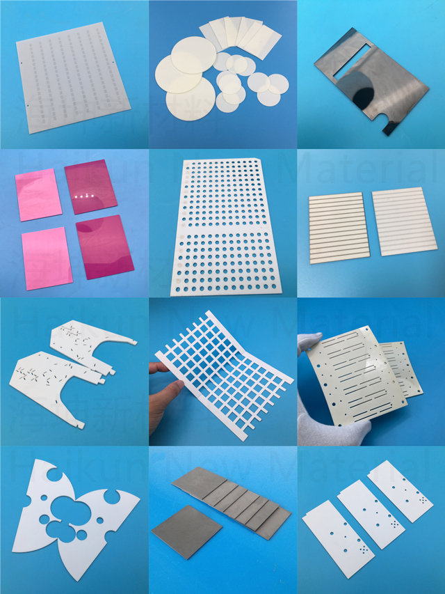
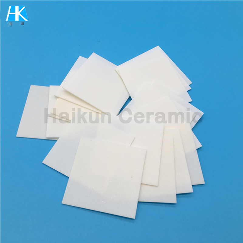
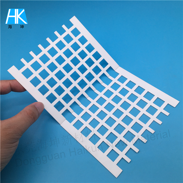
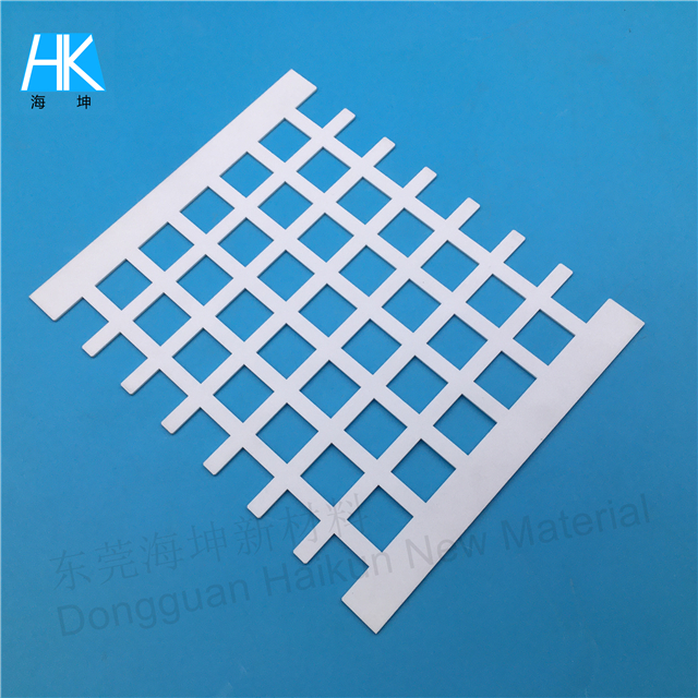
Custom Laser Cut Alumina Ceramic Substrates Manufacturer
Aliases:Precision-Cut Alumina Substrates with Custom Shapes, Fine Features and Dimensional Accuracy.
Introduction
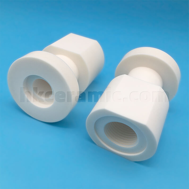
Custom laser cut alumina ceramic substrates for electronic insulation and industrial applications. Available in customized shapes, sizes and thicknesses.
Contact Us
Live
E-mail:sales01@hkceramic.com
Commission
Processing by sample | Processing by drawing | Quote within 3 hours | Samples in 3-10 days
Custom Laser Cut Alumina Ceramic Substrates Manufacturer
*Some content and parameters are for reference only. Our company can adjust ceramic performance and customize processing according to customer needs.
Design Features
1. Advantages of Laser Cutting Technology — Precision Down to the Finest Detail
We utilize high-energy-density, low-heat-input laser systems, enabling exceptional processing precision while maintaining the structural integrity of the material:
Cutting Thickness Range: 0.1–9 mm
Suitable for a full spectrum of thicknesses, from ultra-thin ceramic substrates to high-strength structural components.Cutting Precision: ±0.02 mm
Facilitates tighter structural tolerances for microelectronics and high-precision packaging.Minimum Feature/Hole Size: 0.04 mm
Capable of executing complex processes such as micro-hole arrays, micro-vias, and micro-structured slots.Kerf Width: 0.04 mm
An ultra-narrow cut minimizes material loss and ensures clean, chip-free edges.
Laser micro-machining enables the creation of complex contours that are unattainable with traditional mechanical tools; it is ideal for high-frequency ceramic circuits, sensor substrates, and precision micro-structured components.
2. Precision Lapping and Polishing — Achieving a Mirror-Like Surface Finish
Following laser cutting, Haide employs high-precision double-sided lapping and polishing processes to achieve the following:
Surface roughness (Ra) ≤ 0.1 μm
Meets the requirements for processes such as thick-film printing for microcircuits, thin-film metallization, and chip mounting.Thickness tolerance: ±0.02 mm
Ensures high batch-to-batch consistency, making it ideal for automated assembly and precision stacked structures.
Superior flatness enhances the stability and reliability of ceramic substrates during packaging, heat dissipation, and circuit routing.
3. Excellent Electrical Insulation and Dielectric Properties — Suited for High-Frequency and High-Voltage Applications
Alumina ceramics offer robust insulation and high dielectric stability, making them well-suited for high-frequency, high-voltage, and precision control systems:
Volume resistivity: >10¹⁴ Ω·cm
Dielectric constant: 9–10 (εr)
Dielectric breakdown strength: ≥25 kV/mm
Whether used in RF antennas, power electronics modules, or high-voltage ignition systems, these ceramics provide reliable dielectric isolation and signal stability.
4. High Thermal Conductivity and Thermal Stability — Providing Reliable Heat Dissipation for Power Devices
Thermal Conductivity: 25 W/(m·K) (96% Alumina)
Coefficient of Thermal Expansion: 6.5×10⁻⁶/℃
Maximum Operating Temperature: 1600℃
In environments characterized by high power density or periodic thermal shock, ceramic substrates maintain thermal stability and dimensional consistency, making them critical materials for IGBTs, power modules, and LED packaging.
5. Enhanced Mechanical Properties — Stable Load-Bearing for Demanding Systems
Alumina ceramics offer a combination of high strength and lightweight characteristics:
Flexural Strength: ≥ 300 MPa
Compressive Strength: ≥ 2000 MPa
Vickers Hardness: 1600 HV
Density: 3.7–3.9 g/cm³
Suitable for applications involving high-speed impact, vibration, or heavy-load support—such as precision support structures and sealed baseplates.
Application Areas
1. Electronic Packaging Substrates
Insulating substrates for power modules (IGBT, MOSFET)
Multilayer ceramic circuit boards (LTCC/HTCC)
Carriers for RF/microwave devices
2. Semiconductor Manufacturing
Wafer processing carrier rings
Plasma etching fixtures
High-temperature process trays
3. New Energy Sector
Bipolar plates for fuel cells
Substrate materials for lithium-ion battery separator coatings
Heat-dissipating substrates for photovoltaic inverters
4. Specialized Sensors
Substrates for high-temperature pressure sensors
Support platforms for MEMS devices
Reflective substrates for optical inspection
As a professional manufacturer of ceramic components, we offer custom alumina substrates with purity levels ranging from 95% to 99.9%. We are capable of producing substrates in sizes up to 600×600 mm and provide metallization services—such as copper cladding, gold plating, or the application of molybdenum-manganese layers—tailored to specific requirements. Through optimized material formulations and innovative structural design, our ceramic substrate solutions have been successfully deployed in cutting-edge applications, including 5G base station power amplifiers, electronic control systems for electric vehicles, and satellite payloads. We consistently provide the foundational materials necessary for our clients to achieve device miniaturization, higher power density, and reliable operation at elevated temperatures.
Dongguan Haikun New Material Co., Ltd.
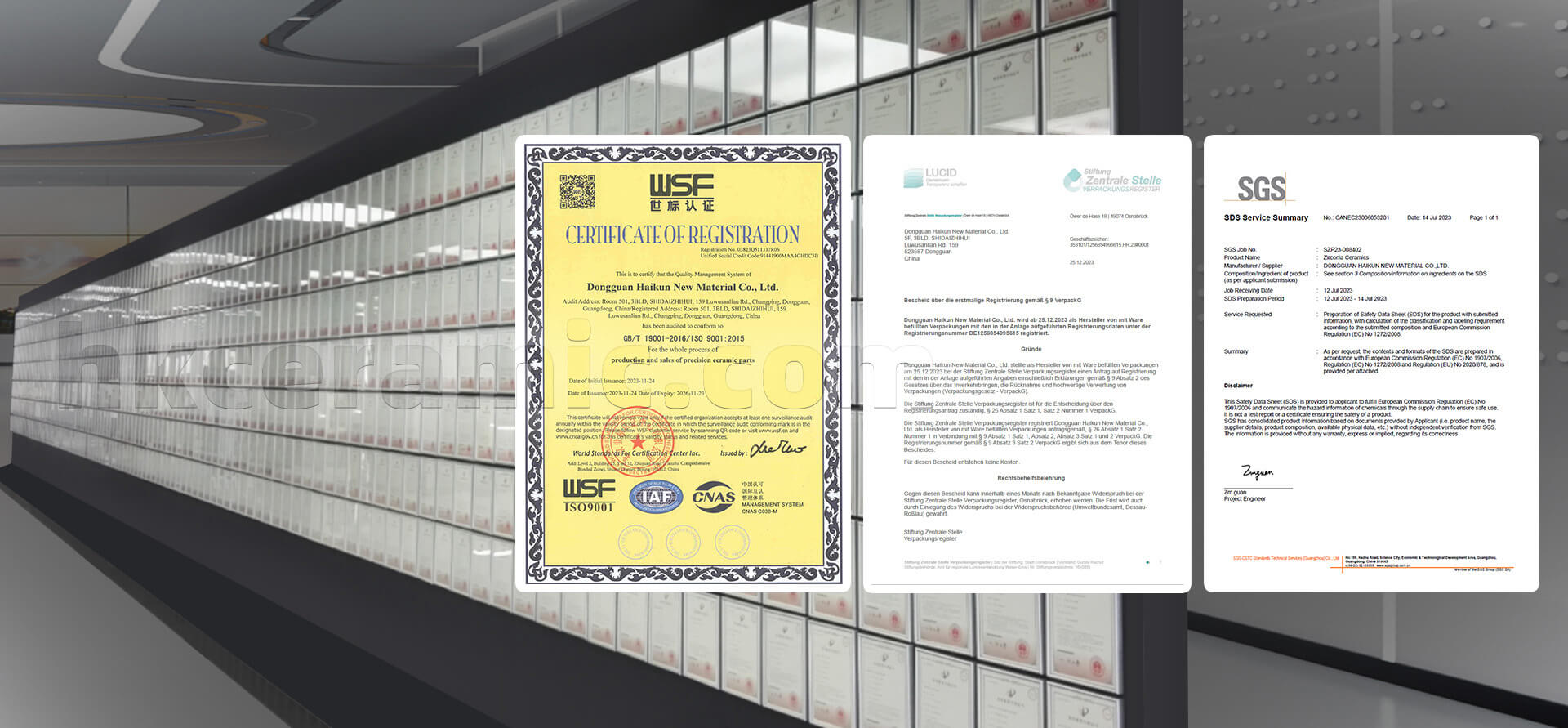
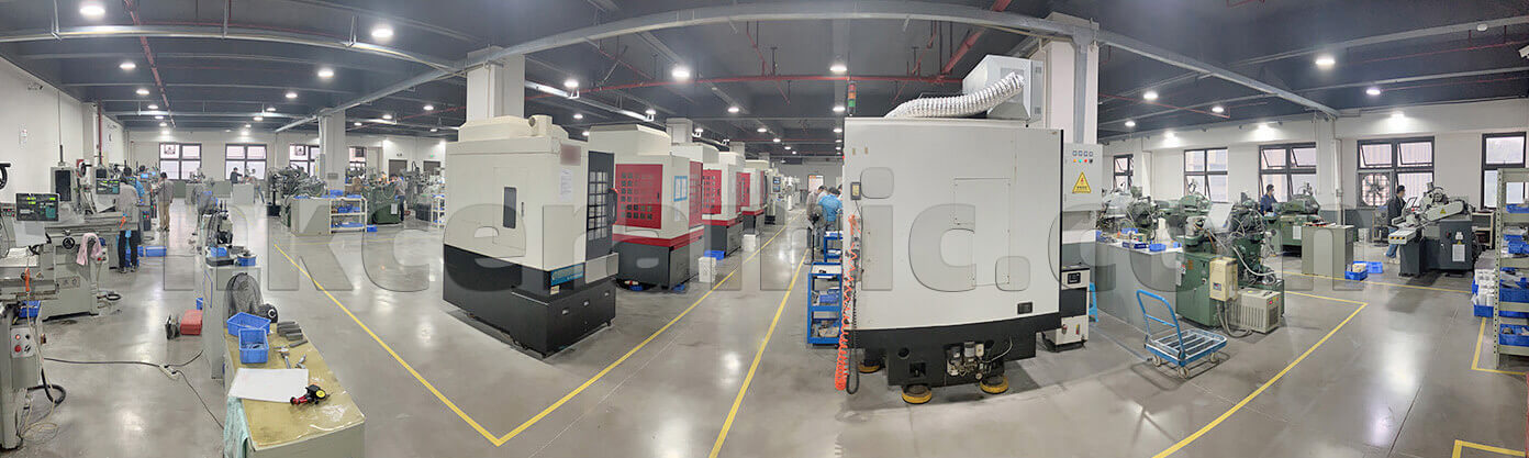
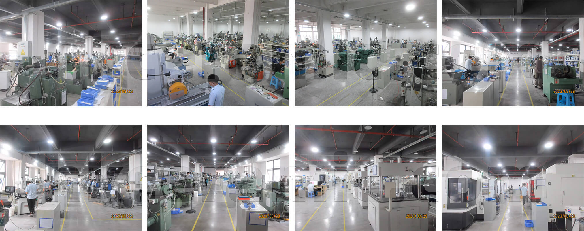
A global advanced precision ceramics (special ceramics) manufacturer, focusing on the development, design, production and sales of advanced precision ceramic products, covering zirconium oxide, aluminum oxide, silicon nitride and other materials, which are widely used in aviation, aerospace, military industry, medical and other fields
0+yr
Industry Experience
0+
Technical Team
0+
Clients
0
Manufacturing Bases
Comparison of ceramic material properties
Not sure which ceramic material is right for your application?
Use our interactive ceramic material comparison chart to compare ceramic materials across different material properties.
Use our interactive ceramic material comparison chart to compare ceramic materials across different material properties.
Click the Property Button above to view the corresponding property comparison of precision ceramic materials
*The values in the table are typical material properties
Precision ceramic product customization process
Step 1
Contact us
Step 2
Technology Assessment
Step 3
Confirm the quotation
Step 4
Signing the contract
Step 5
Inspection and delivery
Step 6
Confirm Receipt